III-V Semiconductor Devices
Performance Beyond Silicon
When traditional materials reach their limits, III-V semiconductors offer a path forward.
Known for their speed, efficiency, and optoelectronic capabilities, they can power everything from high-frequency communication to advanced photonics.
What Sets III-V Apart
Most importantly, they enable faster signal transmission and more efficient light interaction than traditional silicon. Their tunable bandgaps and superior mobility help engineers design devices that push speed, frequency, and photonic efficiency to new heights.
Advanced structures like quantum wells and superlattices add even more control, allowing engineers to tailor performance at the nanoscale.
When III-V Is the Material of Choice
III-V semiconductors make all the difference in process that include:
- Designing RF and microwave systems where high-speed, low-loss performance is critical
- Developing LEDs, lasers, or photodetectors that rely on efficient light emission or absorption
- Building high-performance ICs that need speed & density beyond what silicon can deliver
Veeco: Precision. Quality. Repeatability.
We support the full spectrum of III-V device development, from early-stage research to high-volume production. Whether building complex heterostructures or scaling up a proven process, Veeco gives engineers the control they need to move fast and build with confidence.
The Veeco/CNT Fiji® has been at the forefront of recent advances in III-V devices. This includes deposition of III-V materials like AlN, InN and GaN via atomic layer epitaxy (ALE), epitaxial growth of device quality ternary compounds like AlxGa1-xN and InlxAl1-xN, deposition of buffer layers to enable hetero-epitaxy and growth of gate dielectrics and passivation layers.
ALD enabled III-V devices: Epitaxial growth, multicomponent films, passivation layers
Epitaxial growth of device quality AlN [2], InN [1] and GaN [3] has recently been demonstrated in an Veeco/CNT Fiji®. In Fig.1 below, HRTEM and IFFT confirms crystalline InN aligned with a-sapphire. Fig.2 shows the high quality of AlN grown on GaN – the FWHM of the rocking curve is 670 arc sec for a 37nm film – this is comparable to 1.6μm grown by MBE (420 arc sec) .
High Electron Mobility Transistor is based on formation of a high mobility 2D electron gas at interface between lattice-matched semiconductors. Table-1 shows low carrier concentration and high mobility in an all ALD HEMT device (ALE GaN/ALE AlGaN/ALD Al2O3) indicating the presence of the 2D electron gas. Additionally, HEMT device performance improvement has been shown [5] due to surface passivation by ALE-AlN. Hybrid graphene/III-N heterostructures have been grown [6] enabled by the low temperature of ALD which preserves the surface functionalization of graphene.
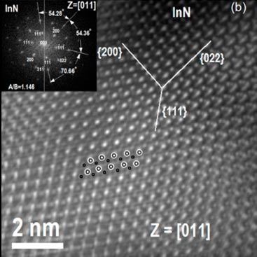
Figure 1: InN on sapphire [1]
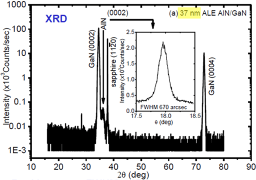
Figure 2: Peaks from AlN/GaN/a-sapphire [2]
ALD Benefits for III-V Devices
- Low deposition temperature
- Ease of growth of alloys including phases not accessed previously
- Deposition on 3D structures like nano-wires
Table-1: HEMT devices via ALD/ALE [4]
| Sample |
μ (cm2/V-s) |
Ns (cm-2) |
| AlGaN / GaN |
1042 |
1.6 x 10¹² |
| Al2O3 / Al0.27Ga0.73N / GaN |
871 |
6.0 x 10¹¹ |
REFERENCES – Recent publications done on Veeco CNT ALD platforms
- Nepal, N., Anderson, V. R., Hite, J. K. & Eddy, C. R., Jr. Growth and Characterization of III-N Ternary Thin Films by Plasma Assisted Atomic Layer Epitaxy at Low Temperatures. Thin Solid Films 1–17 (2015). doi:10.1016/j.tsf.2015.04.068
- Ozgit-Akgun, C. et al. Fabrication of flexible polymer–GaN core–shell nanofibers by the combination of electrospinning and hollow cathode plasma-assisted atomic layer deposition. J. Mater. Chem. C (2015). doi:10.1039/C5TC00343A
- Altuntas, H., Ozgit-Akgun, C., Donmez, I. & Biyikli, N. Current transport mechanisms in plasma-enhanced atomic layer deposited AlN thin films. J Appl Phys 117, 155101 (2015).
- OConnor, E. et al. Effect of forming gas annealing on the inversion response and minority carrier generation lifetime of n and p-In0.53Ga0.47As MOS capacitors. Microelectron Eng (2015). doi:10.1016/j.mee.2015.04.103
- Kao, E., Yang, C., Warren, R., Kozinda, A. & Lin, L. ALD titanium nitride coated carbon nanotube electrodes for electrochemical supercapacitors. TRANSDUCERS 2015 – 2015 18th International Solid-State Sensors, Actuators and Microsystems Conference 498–501 (2015). doi:10.1109/TRANSDUCERS.2015.7180969
- Haider, A., Ozgit-Akgun, C., Goldenberg, E., Okyay, A. K. & Biyikli, N. Low-Temperature Deposition of Hexagonal Boron Nitride Via Sequential Injection of Triethylboron and N 2/H 2Plasma. J Am Ceram Soc n/a–n/a (2014). doi:10.1111/jace.13213
- Assaud, L., Pitzschel, K., Hanbucken, M. & Santinacci, L. Highly-Conformal TiN Thin Films Grown by Thermal and Plasma-Enhanced Atomic Layer Deposition. ECS Journal of Solid State Science and Technology 3, P253–P258 (2014).
- Koehler, A. D., Nepal, N., Anderson, J. T., Hobart, K. D. & Kub, F. J. Investigation of AlGaN/GaN HEMTs Passivated by AlN Films Grown by Atomic Layer Epitaxy. in 135 (2013).
- Ozgit-Akgun, C., Donmez, I. & Biyikli, N. (Invited) Plasma-Enhanced Atomic Layer Deposition of III-Nitride Thin Films. ECS Transactions 58, 289–297 (2013).
- Eddy, C. R., Jr, Nepal, N., Hite, J. K. & Mastro, M. A. Perspectives on future directions in III-N semiconductor research. Journal Of Vacuum Science & Technology A-Vacuum Surfaces And Films 31, 058501 (2013).
- Nepal, N. et al. Epitaxial Growth of III–Nitride/Graphene Heterostructures for Electronic Devices. Appl Phys Express 6, 061003 (2013).
- Nepal, N. et al. Epitaxial Growth of Cubic and Hexagonal InN Thin Films via Plasma-Assisted Atomic Layer Epitaxy. Cryst Growth Des 13, 1485–1490 (2013).
- Ozgit-Akgun, C., Kayaci, F., Donmez, I., Uyar, T. & Biyikli, N. Template-Based Synthesis of Aluminum Nitride Hollow Nanofibers Via Plasma-Enhanced Atomic Layer Deposition. J Am Ceram Soc n/a–n/a (2012). doi:10.1111/jace.12030<
- Ozgit, C., Donmez, I., Alevli, M. & Biyikli, N. Atomic layer deposition of GaN at low temperatures. J Vac Sci Technol A 30, (2012).
- Biyikli, N., Ozgit, C. & Donmez, I. Low-Temperature Self-Limiting Growth of III-Nitride Thin Films by Plasma-Enhanced Atomic Layer Deposition. Nanosci Nanotechnol Lett4, 1008–1014 (2012).
- Ozgit, C., Donmez, I., Alevli, M. & Biyikli, N. Atomic layer deposition of GaN at low temperatures. J Vac Sci Technol A 30, 01A124 (2012).
- Alevli, M., Ozgit, C., Donmez, I. & Biyikli, N. Structural properties of AlN films deposited by plasma-enhanced atomic layer deposition at different growth temperatures. phys. stat. sol. (a) 209, 266–271 (2011).
- Alevli, M., Ozgit, C., Donmez, I. & Biyikli, N. The influence of N2/H2 and ammonia N source materials on optical and structural properties of AlN films grown by plasma enhanced atomic layer deposition. J Cryst Growth 335, 51–57 (2011).
- Alevli, M., Ozgit, C. & Donmez, I. The Influence of Growth Temperature on the Properties of AlN Films Grown by Atomic Layer Deposition. ACTA PHYSICA POLONICA A (2011).
- Ozgit, C., Donmez, I. & Biyikli, N. Self-Limiting Growth of GaN at Low Temperatures. ACTA PHYSICA POLONICA A (2011).