ALD for highly controllable thin films
- Film thickness based on self-limiting, self assembled behavior, with nanometer level control
- Stoichiometric control of multicomponent films
- Films/Processes scalable over very large areas
- Excellent repeatability
- Wide process windows (with respect to temperature or precursor dose variations)
- Low defect density
- Amorphous or crystalline film types depending on substrate and temperature
- Fine control of multilayer coatings, heterostructures, nanolaminates, mixed oxides, graded index layers, and doping
- Standard recipes available for oxides, nitrides, metals, and semiconductors
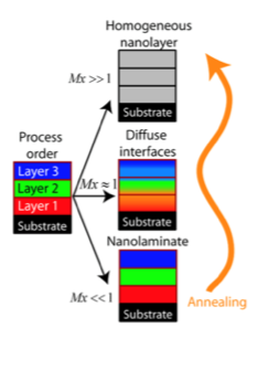
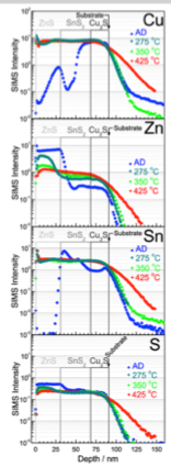
Cu2S/SnS2/ZnS trilayer deposited in silicon trench. CZST film composition profile is analyzed by SIMS following different thermal anneals.
Ref: Thimsen et al, Chemistry of Materials, 24 (16), 3188-3196 (2013). doi:10.1021/cm3015463
ALD for highly controllable thin films
- Excellent conformality, 100% step coverage: uniform coatings on flat, inside porous, and around particle samples
- Atomically flat and smooth coating that conforms to the substrate geometry
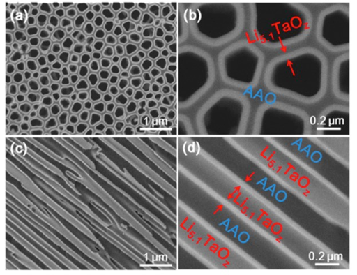
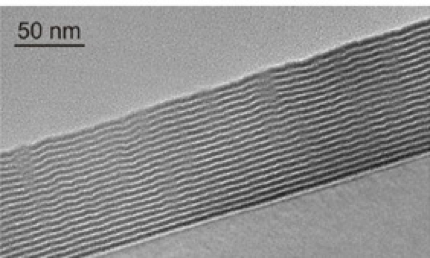
Conformal deposition of Li5.1TaOz deposited by ALD in 300:1 AAO nanotemplate (470:1 final AR)
Ref: Liu, J. et al., J. Phys. Chem. C 117, 20260–20267 (2013).
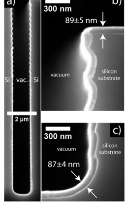
ALD for challenging substrate
- Gentle deposition process for sensitive substrates
- Low temperature deposition possible (RT-800 °C)
- Low power plasma processing (as low as 20-50W) capability
- Coatings demonstrated on polymers, OLEDs, and noble metal surfaces
- Excellent adhesion due to chemical bonds at the first layer
- Low stress due to molecular self-assembly
Al2O3 – ZrO2 nanolaminate encapsulation with a water transmission rate (WVTR) of 5E-7g/m2/day at room temperature – deposited in Savannah® at 80˚C
Ref: Meyer, J., et al. (2009). Applied Physics Letters, 94(23), 233305