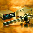
UNI-Bulb RF Plasma Source for Oxygen, Nitrogen and Hydrogen
Optimize Production of Electronic and Optoelectronic Devices

Get optimal conditions for GaN growth of electronic and optoelectronic materials, plus unrivaled plasma stability and reproducibility, with Veeco’s Uni-Bulb RF Plasma Source. One-piece PBN gas inlet tube and plasma bulb combines with dual coaxial RF coil for excellent power coupling and heat removal. Several design options, including customized aperture plates, are available to enhance performance further.
A gas plasma is an effective tool for conversion of highly stable source gases such as N2 or H2 to more active atomic and molecular species suitable for MBE growth. The Veeco UNI-Bulb features a patented one-piece PBN gas inlet tube and plasma bulb to eliminate gas leakage around the bulb. The resulting plasma is highly stable and reproducible, allowing many hours of run time without source re-tuning.
Interchangeable aperture plates are available in configurations of varying gas conductance for growth of GaN, mixed As/N materials, nitrogen doping, hydrogen cleaning and hydrogen assisted growth. The exit hole design minimizes ion content in the beam, while the active neutral species (atomic and molecular) are directed toward the substrate. Customized high uniformity aperture plates are available for most commercial MBE systems enabling typical uniformity of ±1%.
- Patented design with more than 225 in the field
- All-PBN, oxide-free plasma bulb construction
- Optimized exit aperture minimizes ion content and provides excellent film uniformity
- Excellent plasma stability and reproducibility
- Configurations available for growth of GaN, mixed nitrides, N doping, hydrogen cleaning and hydrogen assisted growth
- Autotuner option ensures stable growth conditions and optimizes power efficiencies
Performance and Benefits
The Veeco UNI-Bulb RF Plasma Source is the world’s most popular for nitride growth by MBE. It provides optimal conditions for nitride growth, as proven by its record-setting results for electronic and optoelectronic applications.
These include:
- Record low threshold currents for 1.32μm GaInNAs/GaAs quantum well lasers (Tampere University of Technology, 2001)
- Production of 1.26μm InGaAsN VCSELs compatible with telecom network requirements (Cielo Communications and Sandia National Laboratories, 2001)
- Growth of AlGaN/GaN two-dimensional electron gas structures with record high mobility’s of 160,000cm2/Vsec at 77K and 51,700cm2/Vsec at 13K (University of California, Santa Barbara, 1999)
- PI-HEMTs from AlGaN/GaN show small signal RF performance and DC breakdowns as a function of gate length that are as good as the best transistors made by MOVPE (Cornell University, 1999)
- Reported GaN growth rates as high as 2.6μm/hr. (University of Tokyo, 1999). Most commonly, the source is used for GaN growth rates in the range of 0.8-1.0μm/hr
- Mass spectroscopy studies indicate that the beam flux is rich in metastable nitrogen molecules with very low ion content. The metastable molecules exhibit a high incorporation rate in GaN growth and stabilize the growth rate at high substrate temperatures (approx. 700-750°C.) (West Virginia University, 1999)