EpiStride CVD System for SiC Epitaxy
Introducing EpiStride CVD System for Silicon Carbide Epitaxy
- Veeco’s latest technology for the compound semiconductor market
- Horizontal flow, hot wall chemical vapor deposition (CVD) system for Silicon Carbide (SiC) epitaxy
- Single-wafer reactor capable of processing wafers of any size up to 200mm
- Available in single- or dual-chamber configurations
- Powerful platform designed for cutting-edge silicon carbide R&D
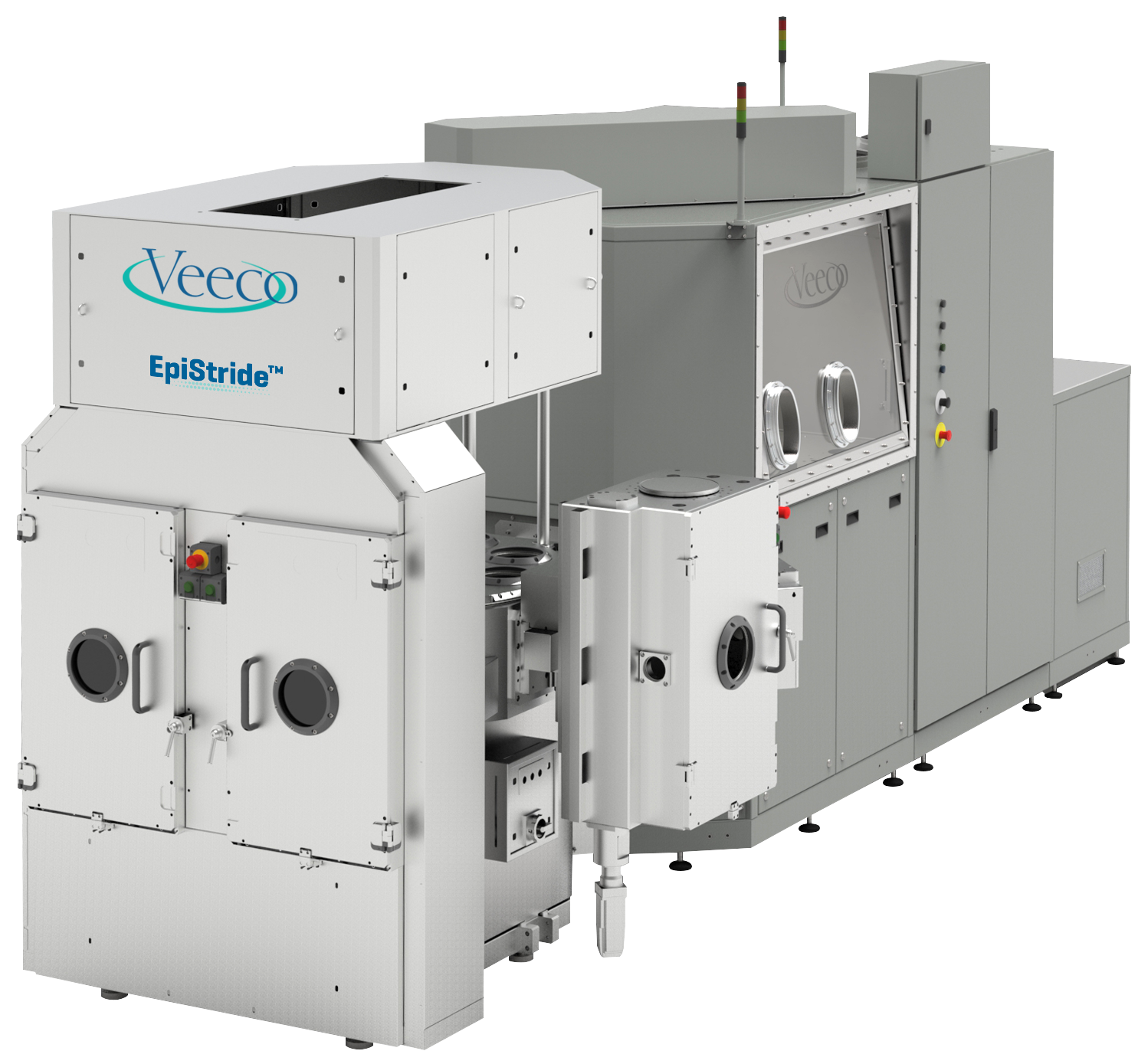
EpiStride SiC CVD System – single reactor configuration
Epitaxial Quality
- Thickness uniformity <1% and doping uniformity below 2% for 10-15um thick epitaxial layers
- Repeatable and reliable quality throughout an entire campaign cycle between maintenance events
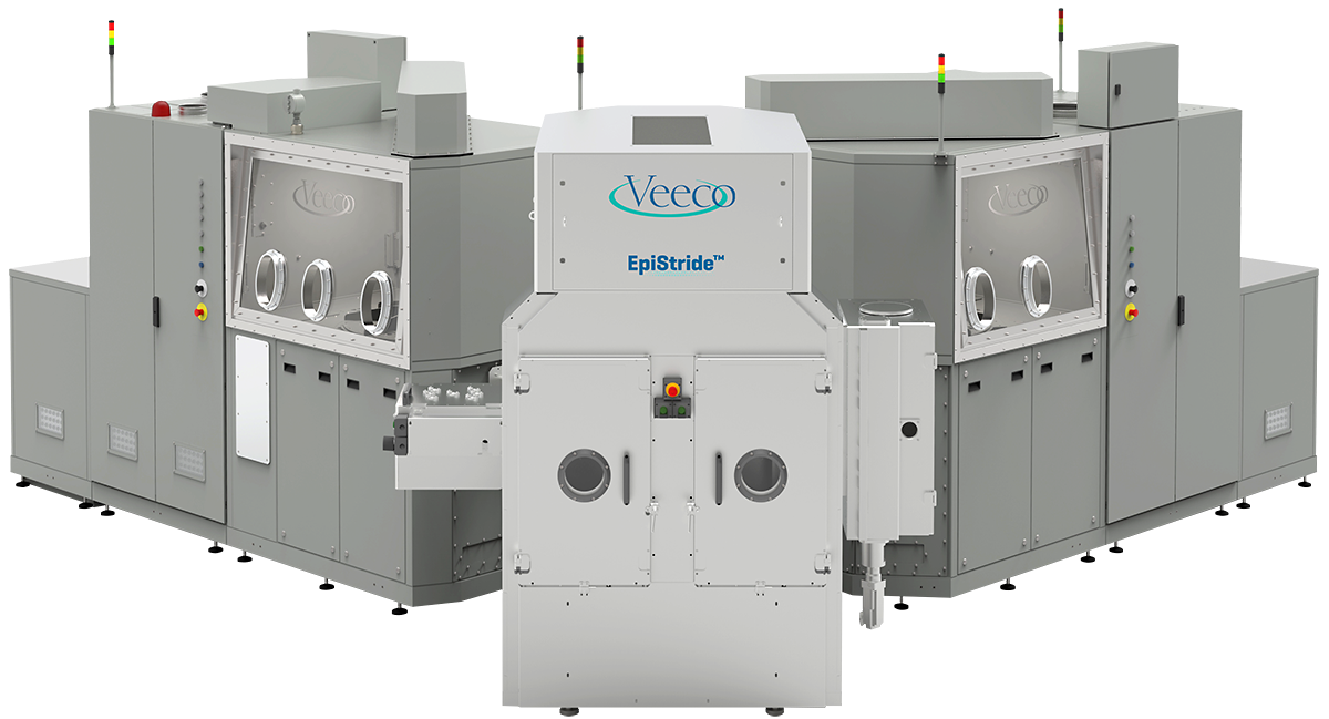
EpiStride SiC CVD System – dual reactor configuration
Ease of Use
- EpiStride is the only system in the industry that can complete routine cleaning maintenance in
less than 5 hours (green-to-green time), with total human touch-time reduced to less than 1 hour - Routine cleaning maintenance is performed in an inert environment through a glovebox with easy access to the reactor’s growth cell
- EpiStride’s glovebox allows for a quick exchange of parts without complex and time-consuming disconnection of hardware components
- Upon maintenance completion, EpiStride immediately achieves baseline performance without further hardware or software tuning
Broad Process Window
EpiStride’s approach to temperature and gas flow accelerates process development and improves the repeatability of results.
6 Independent Heating Zones
- EpiStride is the only system that utilizes individually controlled heater zones to tune and
optimize the temperature profile of the growth chamber - The six independent heating zones enable better control of wall temperature upstream and
downstream of the wafer as well as control of vertical temperature gradients - These tuning knobs lead to better temperature uniformity at the wafer surface
3-Zone Gas Injector
- EpiStride’s 3-zone injector allows adjustments of gas concentrations and flows between the center
and the edges of the wafer which can lead to better doping uniformity across the wafer - The flow of nitrogen dopant can be adjusted only on the side channels to offset the off-gassing of
parasitic deposition near the growth cell sidewalls - Other possible uses include varying the Carbon-to-Silicon ratio between the center and the edge
channels as well as varying the amount of carrier gas flowing through different channels
Next Generation Capabilities
- EpiStride’s optional 2-reactor configuration can run different dopants (n and p) in separate chambers to build bipolar epi layers without extensive maintenance to change dopants
- The second chamber can also be configured for different materials such as Gallium Nitride (GaN) for exploration of composite epi layers
- Separate pre-heating and cooldown stations reduce extreme thermal cycling shocks on the wafer